


- Description
Description
1206 SMD Silicon Photodiode Overview
The JC1206PD0224 is a compact 1206 SMD silicon photodiode designed for optical detection and infrared sensing. The device combines high photosensitivity and fast response in a surface-mount package suitable for compact PCB integration.
The photodiode uses silicon die material and a water-clear lens. According to the datasheet, typical applications include infrared applied systems, optoelectronic switches and smoke alarms.
Key Features
- 1206 SMD photodiode
- Silicon die material
- High photosensitivity
- Fast response time
- Water-clear lens
- Minimum 33V reverse breakdown voltage
- Maximum 10nA reverse dark current
- Typical total capacitance: 1pF
- Pb-free construction
- Compliant with EU RoHS requirements
- Tape-and-reel packaging for automated assembly
Product Specifications
| Parameter | Specification |
|---|---|
| Model | JC1206PD0224 |
| Product Type | 1206 SMD Photodiode |
| Die Material | Silicon |
| Lens Color | Water Clear |
| Reverse Voltage | 33 V |
| Reverse Breakdown Voltage | Min. 33 V |
| Reverse Dark Current | Max. 10 nA |
| Open Circuit Voltage | Typ. 390 mV |
| Short Circuit Current | Typ. 2 µA |
| Reverse Light Current | Typ. 2 µA |
| Total Capacitance | Typ. 1 pF |
| Power Consumption | 150 mW |
| Operating Temperature Range | -25°C to +85°C |
| Storage Temperature Range | -40°C to +100°C |
| Compliance | Pb-free / RoHS compliant |
Detailed Electrical Characteristics
The following detailed electrical characteristics are specified at Ta = 25°C. Test conditions are retained from the original datasheet without altering the source values.
| Parameter | Symbol | Condition | Min. | Typ. | Max. | Unit |
|---|---|---|---|---|---|---|
| Reverse Dark Current | ID | VR = 10V, Ee = 0mW/cm² | — | — | 10 | nA |
| Reverse Breakdown Voltage | V(BR)R | IR = 100µA, Ee = 0mW/cm² | 33 | — | — | V |
| Open Circuit Voltage | Voc | T = 2856K, Ee = 5mW/cm² | — | 390 | — | mV |
| Short Circuit Current | Isc | T = 2856K, Ee = 5mW/cm² | — | 2 | — | µA |
| Reverse Light Current | IL | VR = 5V, T = 2856K, Ee = 5mW/cm² | — | 2 | — | µA |
| Total Capacitance | CT | VR = 5V, Ee = 0mW/cm², f = 1MHz | — | 1 | — | pF |
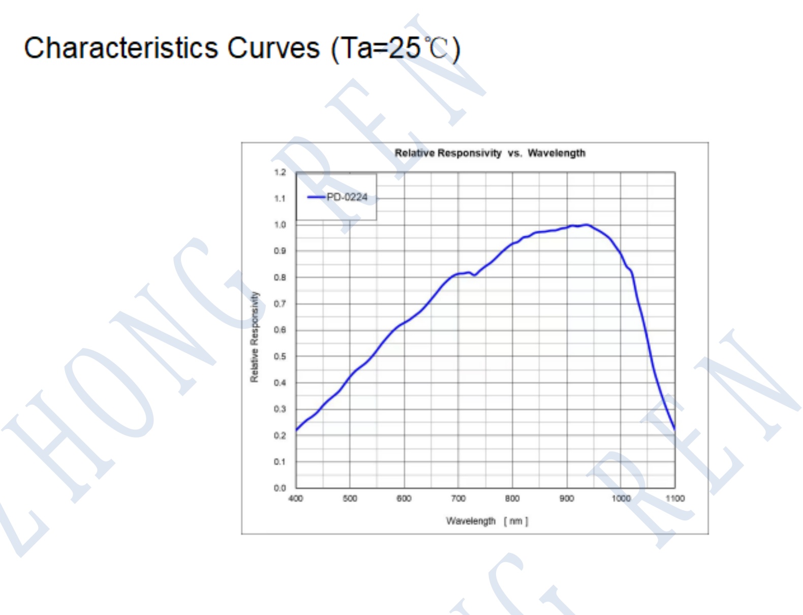
Relative Spectral Responsivity
The datasheet provides a Relative Responsivity vs. Wavelength characteristic curve at Ta = 25°C. The plotted response increases through the visible and near-infrared region, reaches its highest relative responsivity in the near-infrared portion of the chart, and then decreases toward the long-wavelength end of the plotted range.
The curve should be used as a typical characteristic reference rather than interpreted as a guaranteed minimum or maximum spectral response specification.
Absolute Maximum Ratings
| Symbol | Parameter | Rated | Unit |
|---|---|---|---|
| VR | Reverse Voltage | 33 | V |
| PM | Power Consumption | 150 | mW |
| Top | Operating Temperature Range | -25 to +85 | °C |
| Tstg | Storage Temperature Range | -40 to +100 | °C |
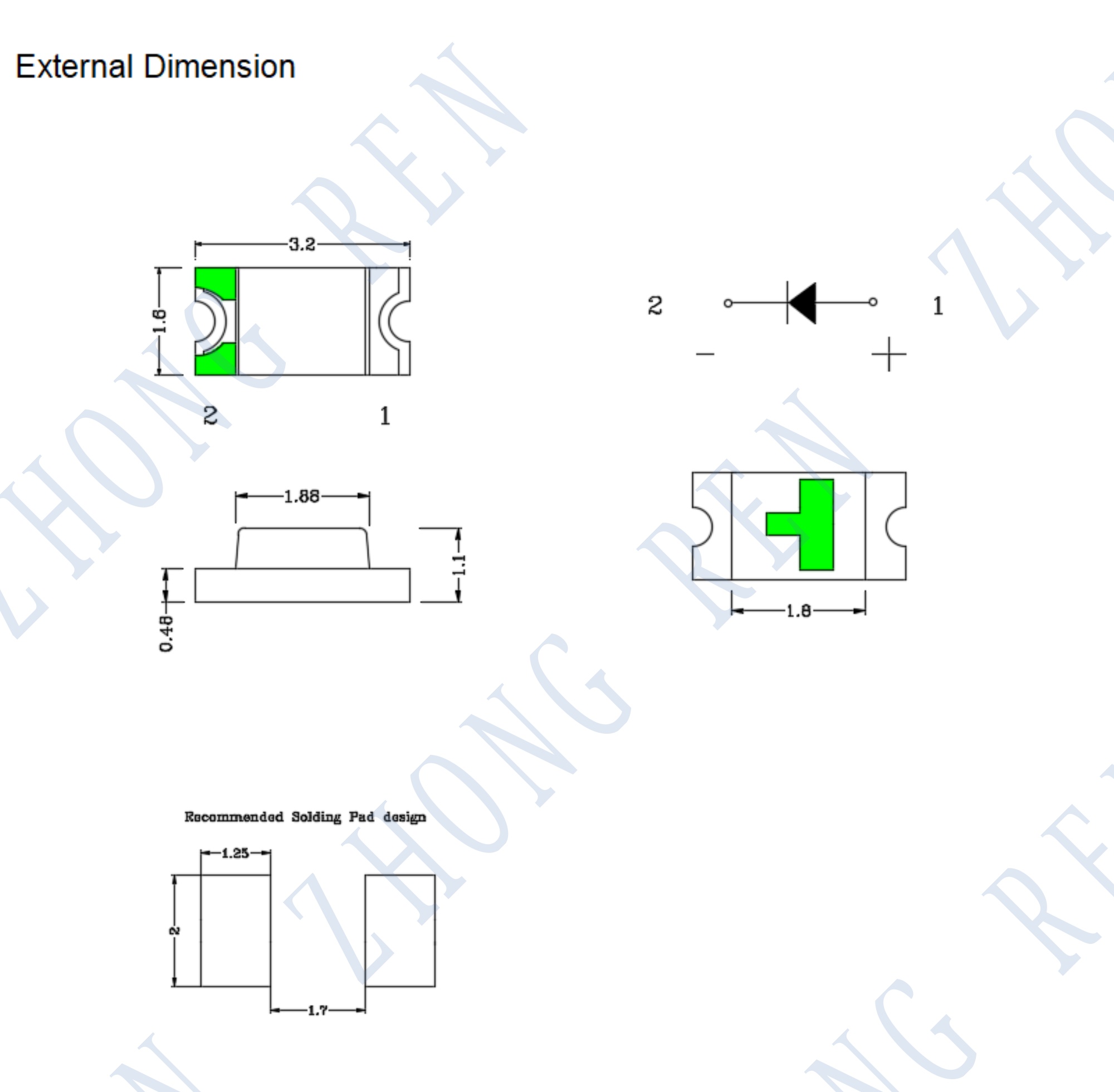
1206 SMD Package Dimensions
The JC1206PD0224 is supplied in a compact 1206 surface-mount package. The original dimensional drawing provides package dimensions, device polarity and the recommended PCB soldering pad layout.
| Package Parameter | Dimension |
|---|---|
| Package Length | 3.2 mm |
| Package Width | 1.6 mm |
| Lens Width | 1.88 mm |
| Overall Height | 1.1 mm |
| Base Height | 0.48 mm |
Typical Applications
The original datasheet lists the JC1206PD0224 for several optical detection applications where a compact silicon photodiode is required.
- Infrared applied systems
- Optoelectronic switches
- Smoke alarms
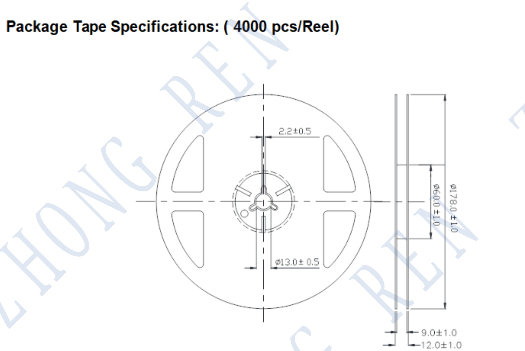
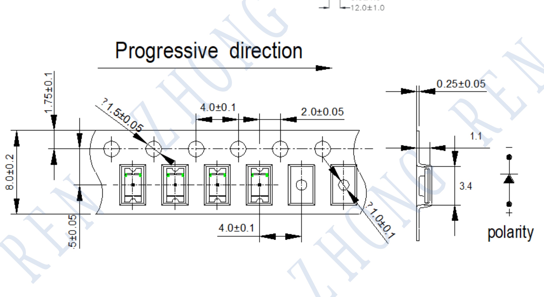
Tape and Reel Packaging
The JC1206PD0224 is supplied in tape-and-reel packaging with 4000 pieces per reel. The original packaging drawing also provides the progressive direction, carrier tape dimensions and photodiode polarity for automated surface-mount assembly.
Storage and Handling
The datasheet specifies moisture-controlled storage and handling requirements before and after opening the package. These requirements should be followed before PCB mounting and soldering.
- Do not open the moisture-proof bag before the devices are ready for use.
- Before opening, store at 30°C or below and 60% RH or below.
- The maximum storage period before opening the package is 1 year.
- After opening, keep the devices at 30°C / 35% RH or below.
- Use the devices within 7 days after opening.
- If baking is required before mounting, use 60 ± 5°C for 12 hours.
Soldering Precautions
Proper handling and soldering conditions are important for maintaining device reliability. The datasheet specifies the following precautions for PCB assembly.
- Use an appropriate current-limiting circuit where required by the application.
- Avoid instantaneous high voltage during circuit turn-on and turn-off.
- Reflow soldering should not be performed more than two times.
- Do not apply mechanical stress to the device during soldering.
- Do not warp the circuit board before it has returned to normal ambient conditions after soldering.
Request a Quote
Contact LumiLaserChip for pricing, samples, lead time and technical information for the JC1206PD0224 1206 SMD silicon photodiode. Please provide your required quantity, target application and relevant optical or electrical requirements when requesting a quotation.
