


- Description
Description
940nm 1616 SMD VCSEL & Photodiode Overview
The 1616VCA940R8-PD0224-Z is an integrated 940nm VCSEL and photosensitive diode device supplied in a compact 1616 SMD package. The VCSEL section is designed for short-range P-sensor applications, while the integrated photodiode provides optical detection functionality within the same surface-mount package.
The device combines a typical VCSEL optical output power of 7.2mW, typical operating current of 10mA, typical forward voltage of 1.8V and typical power conversion efficiency of 40%. The photosensitive diode section provides a maximum reverse dark current of 10nA, minimum reverse breakdown voltage of 33V and typical total capacitance of 1pF.
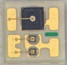
Key Features
- Integrated 940nm VCSEL and photosensitive diode
- Compact 1616 SMD package
- High reliability
- Wavelength stabilization
- Typical VCSEL optical power: 7.2mW
- Typical VCSEL operating current: 10mA
- Typical VCSEL forward voltage: 1.8V
- Typical power conversion efficiency: 40%
- Maximum PD reverse dark current: 10nA
- Minimum PD reverse breakdown voltage: 33V
- Typical PD capacitance: 1pF
- ESD threshold: 8000V, Human Body Model
- Laser Safety Class 1M
- Pb-free and compliant with EU RoHS requirements
- Moisture proof grade: L3
Product Specifications
| Parameter | Specification |
|---|---|
| Model | 1616VCA940R8-PD0224-Z |
| Product Type | 1616 SMD VCSEL & Photodiode |
| VCSEL Wavelength | 940 nm |
| Typical VCSEL Optical Power | 7.2 mW |
| Typical VCSEL Operating Current | 10 mA |
| Typical VCSEL Forward Voltage | 1.8 V |
| Typical VCSEL Divergence | 23° |
| Typical VCSEL PCE | 40% |
| PD Reverse Dark Current | Max. 10 nA |
| PD Reverse Breakdown Voltage | Min. 33 V |
| PD Total Capacitance | Typ. 1 pF |
| Package Size | 1.6 × 1.6 mm |
| Laser Safety | Class 1M |
| Moisture Proof Grade | L3 |
| Compliance | Pb-free / RoHS compliant |
VCSEL Electrical and Optical Characteristics
The following VCSEL characteristics are provided in the original datasheet. The test notes specify measurements at the suggested bias current with the backside of the chip at 50°C under CW operation where applicable.
| Category | Parameter | Symbol | Unit | Min. | Typical | Max. | Notes |
|---|---|---|---|---|---|---|---|
| Electrical | Threshold Current | Ith | mA | — | 1.35 | 2 | #1, #2 |
| Electrical | Operating Current | I0 | mA | — | 10 | — | — |
| Electrical | Forward Voltage | V0 | V | 1.6 | 1.8 | 2.2 | #1 |
| Optical | Central Wavelength | λp | nm | 934 | 940 | 946 | #1 |
| Optical | Divergence | Θ | ° | 20 | 23 | 26 | Full width, 1/e², #1 |
| Optical | Optical Power | Po | mW | 6.5 | 7.2 | 8.5 | Peak, #1 |
| Optical | Dead Emitters | Nde | ea | — | — | 0 | #1, #3 |
| Opti-electrical | Slope Efficiency | ηSE | mW/mA | 0.75 | 0.83 | — | #1, #2 |
| Opti-electrical | Power Conversion Efficiency | PCE | % | 36 | 40 | — | #1 |
VCSEL Specification Notes
- #1: Tested at the suggested bias current, with the temperature on the backside of the chip at 50°C under CW operation.
- #2: Linear regression between 3mA and 6mA.
- #3: Dead emitters are defined as emitters with output power below 50% of the average of all emitters in the unit.
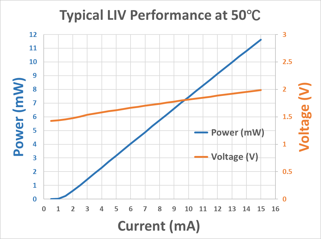
Typical LIV Performance at 50°C
The datasheet provides a typical LIV performance curve at 50°C showing the relationship between current, optical output power and forward voltage. Optical output increases with drive current while forward voltage rises gradually across the plotted operating range.
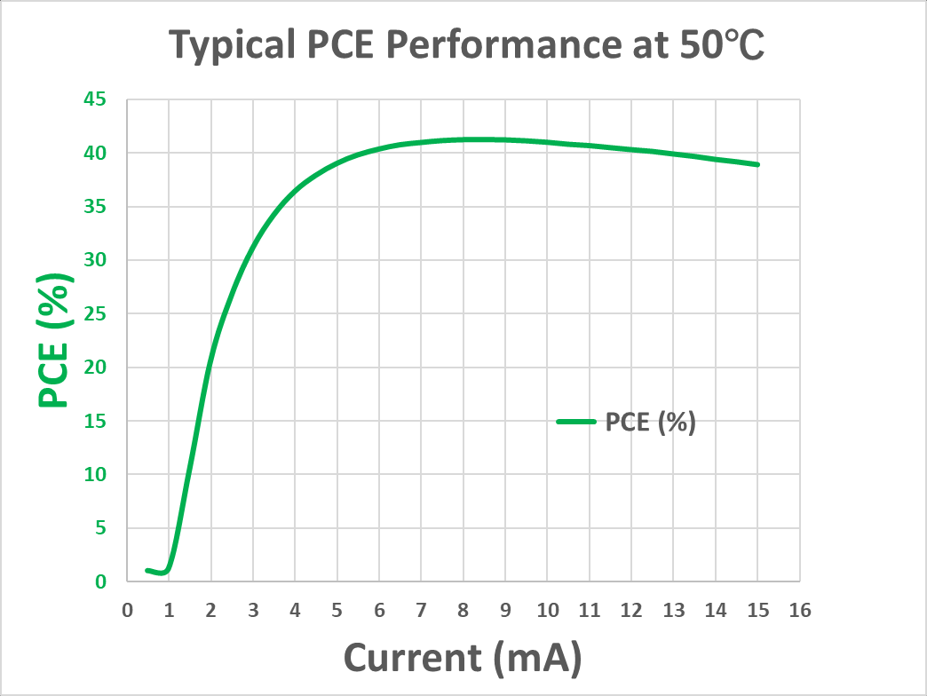
Typical Power Conversion Efficiency
The typical PCE curve in the datasheet shows power conversion efficiency as a function of drive current at 50°C. The detailed specifications list a typical PCE value of 40% under the stated measurement conditions.
Photosensitive Diode Characteristics
The integrated photosensitive diode provides optical detection within the same 1616 SMD package. The following values are specified at Ta = 25°C and are based on 100% probing according to the datasheet.
| Parameter | Symbol | Condition | Min. | Typ. | Max. | Unit |
|---|---|---|---|---|---|---|
| Reverse Dark Current | ID | VR = 10V, Ee = 0mW/cm² | — | — | 10 | nA |
| Reverse Breakdown Voltage | V(BR)R | IR = 100µA, Ee = 0mW/cm² | 33 | — | — | V |
| Open Circuit Voltage | Voc | T = 2856K, Ee = 5mW/cm² | — | 390 | — | mV |
| Short Circuit Current | Isc | T = 2856K, Ee = 5mW/cm² | — | 2 | — | µA |
| Reverse Light Current | IL | VR = 5V, T = 2856K, Ee = 5mW/cm² | — | 2 | — | µA |
| Total Capacitance | CT | VR = 5V, Ee = 0mW/cm², f = 1MHz | — | 1 | — | pF |
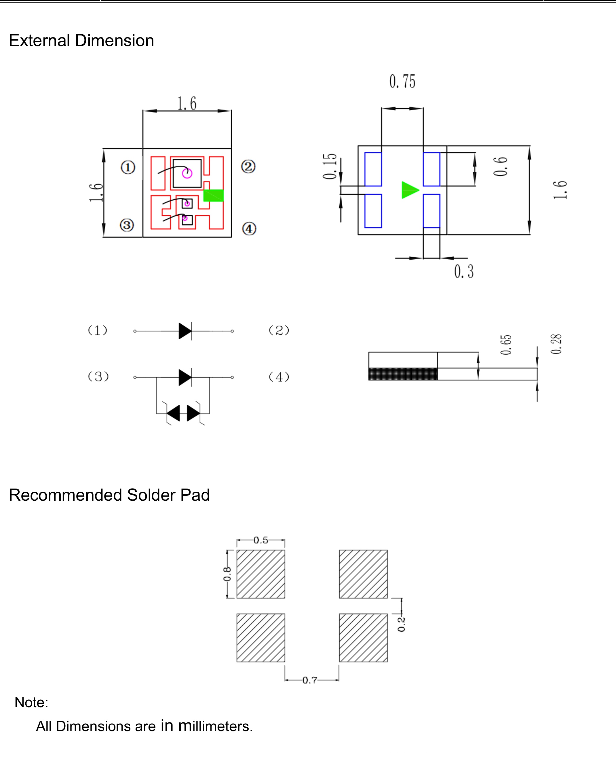
1616 SMD Package and Pin Configuration
The integrated device uses a compact 1.6 × 1.6mm SMD package with four electrical terminals. The original dimensional drawing provides the VCSEL and photodiode circuit configuration together with the recommended PCB solder-pad layout.
VCSEL Absolute Maximum Ratings
| Parameter | Rating |
|---|---|
| Maximum CW Forward Bias Current | 15 mA |
| Maximum Reverse Bias Voltage | 5 V |
| ESD Threshold (Human Body Model) | 8000 V |
| Storage Temperature Range | -40°C to +105°C |
| Substrate Temperature During Operation | -20°C to +85°C |
Laser Safety
The datasheet specifies the device as Laser Safety Class 1M. The product should only be handled by authorized users with appropriate safety precautions. The datasheet further states that laser safety glasses compliant with ANSI Z136 and CE certified should be worn during operation.
Application Fields
The original datasheet lists the following application fields for the 1616VCA940R8-PD0224-Z integrated VCSEL and photodiode device.
- Consumer electronics
- Laser radar
- Machine vision
- Industrial applications
Tape and Reel Packaging
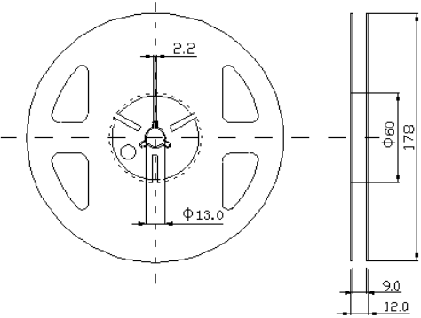
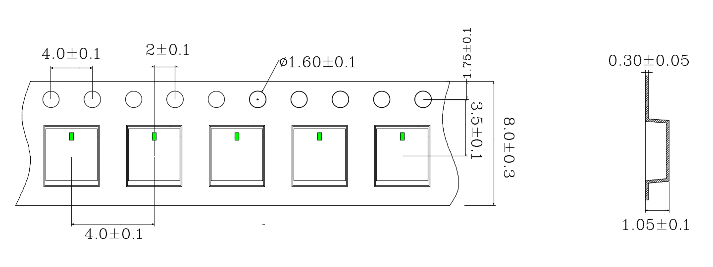
The 1616VCA940R8-PD0224-Z is supplied in tape-and-reel packaging with 4000 pieces per reel. The original packaging drawings provide the reel dimensions, carrier tape dimensions and component orientation for automated surface-mount production.
Storage and Handling
The datasheet specifies moisture-controlled storage requirements before and after opening the packaging. These conditions should be followed before PCB mounting and soldering.
- Do not open the moisture-proof bag before the devices are ready for use.
- Before opening, store at 30°C or below and 60% RH or below.
- The maximum storage period before opening the package is 1 year.
- After opening, keep the devices at 30°C / 35% RH or below.
- Use the devices within 7 days after opening.
- If baking is required before mounting, use 60 ± 5°C for 12 hours.
Soldering Precautions
Proper soldering and electrical handling are important for maintaining device reliability. The datasheet specifies precautions for current limiting, transient voltage protection and reflow soldering.
- Use an appropriate current-limiting resistor so the device remains within the rated current.
- Avoid instantaneous high voltage during circuit turn-on and turn-off.
- Reflow soldering should not be performed more than two times.
- Do not apply mechanical stress to the device during soldering.
- Do not warp the circuit board before it has returned to normal ambient conditions after soldering.
Request a Quote
Contact LumiLaserChip for pricing, sample availability, lead time and technical information for the 1616VCA940R8-PD0224-Z 940nm 1616 SMD VCSEL & Photodiode. When requesting a quotation, please provide your required quantity, target application and relevant optical or electrical requirements for project evaluation.
