


- Description
Description
850nm 1206 SMD VCSEL Overview
The 1206ULM850-L is a single-channel 850nm VCSEL (Vertical-Cavity Surface-Emitting Laser) supplied in a compact 1206 surface-mount package. It provides a typical emission wavelength of 850nm, a typical optical output power of 2mW at IF = 6mA, and a specified peak power of 30mW.
Designed for compact surface-mount integration, the device combines high reliability, wavelength stabilization and high-speed optical performance. It provides a minimum 3dB modulation bandwidth of 3GHz at IF = 6mA and a typical viewing angle of 12°.
Key Features
- 1206 SMD VCSEL package
- Single-channel VCSEL
- Typical emission wavelength: 850nm
- Typical optical output power: 2mW at IF = 6mA
- Specified peak power: 30mW
- Minimum 3GHz modulation bandwidth at IF = 6mA
- High reliability
- Wavelength stabilization
- Pb-free product compliant with EU RoHS requirements
- Moisture proof grade: L3
Product Specifications
| Parameter | Specification |
|---|---|
| Model | 1206ULM850-L |
| Product Type | 1206 SMD VCSEL |
| Channel | Single Channel |
| Typical Wavelength | 850 nm |
| Wavelength Range | 830–860 nm |
| Typical Optical Output Power | 2 mW @ IF = 6 mA |
| Peak Power | 30 mW |
| 3dB Modulation Bandwidth | Min. 3 GHz @ IF = 6 mA |
| Typical Viewing Angle | 12° @ IF = 6 mA |
| VCSEL Chip Dimension | 200 × 200 × 150 µm |
| Moisture Proof Grade | L3 |
| Compliance | Pb-free / RoHS compliant |
Detailed Optical and Electrical Characteristics
The following optical and electrical characteristics are specified at Ta = 25°C, unless otherwise stated in the original product datasheet.
| Parameter | Symbol | Unit | Min. | Typ. | Max. | Test Conditions |
|---|---|---|---|---|---|---|
| Emission Wavelength | λ | nm | 830 | 850 | 860 | IF = 6mA |
| Threshold Current | ITH | mA | 0.40 | 0.90 | 1.40 | — |
| Threshold Current | ITH | mA | 0.40 | — | 2.5 | T = -40–90°C |
| Optical Output Power | Popt | mW | — | 2 | — | IF = 6mA |
| Slope Efficiency | ηS | W/A | 0.27 | — | 0.55 | — |
| Variation of ηS over Temperature | ΔηS / ηS / ΔT | %/K | — | 0.45 | 0.60 | T = -40–25°C / T = 25–90°C |
| Differential Series Resistance | Rs | Ω | 25 | 50 | 65 | IF = 6mA |
| 3dB Modulation Bandwidth | V3dB | GHz | 3 | — | — | IF = 6mA |
| Rise and Fall Time | tR/tF | ps | — | 70 | 80 | 20%–80%; ER = 5dB; IF = 6mA |
| Relative Intensity Noise | RIN | dB/Hz | — | -130 | -120 | IF = 6mA |
| Spectral Width | Δλ | nm | — | 0.30 | 0.65 | IF = 6mA, RMS |
| Viewing Angle | 2θ1/2 | deg | — | 12 | — | IF = 6mA |
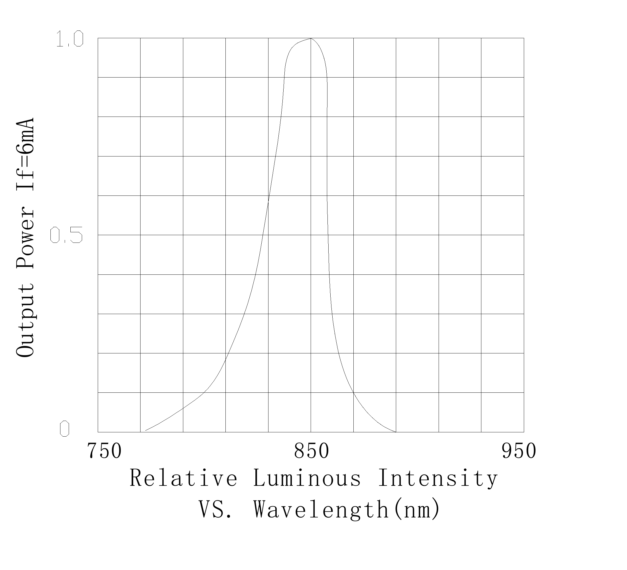
850nm Spectrum Characteristics
The spectrum chart provided in the datasheet shows optical emission centered around the nominal 850nm wavelength. At IF = 6mA, the specified emission wavelength range is 830–860nm, with a typical value of 850nm.
The spectral width is typically 0.30nm and has a specified maximum of 0.65nm at IF = 6mA under the stated RMS measurement conditions.
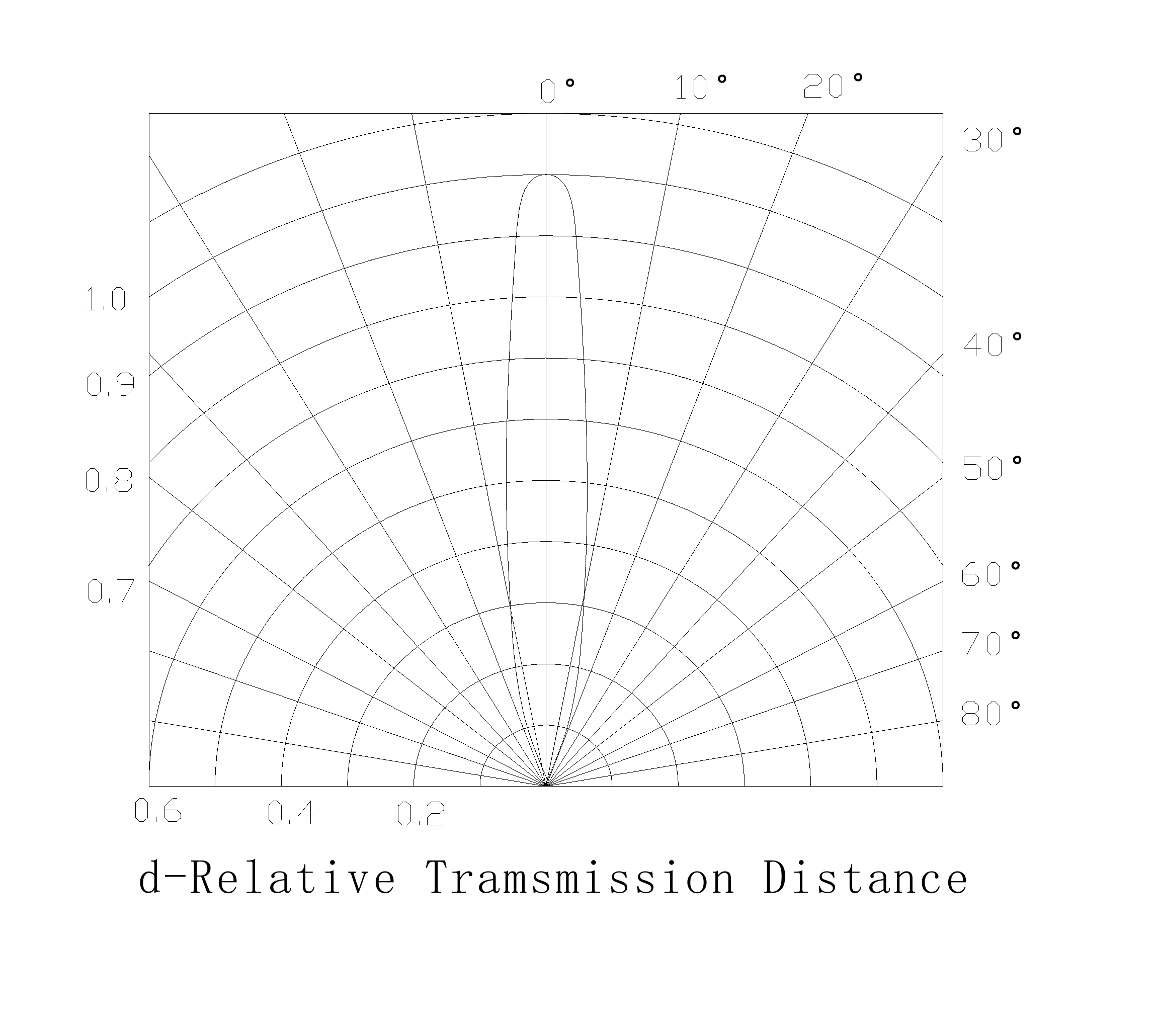
Optical Radiation Pattern
The 1206ULM850-L has a typical viewing angle of 12° at IF = 6mA. The radiation pattern below is extracted directly from the original product datasheet.
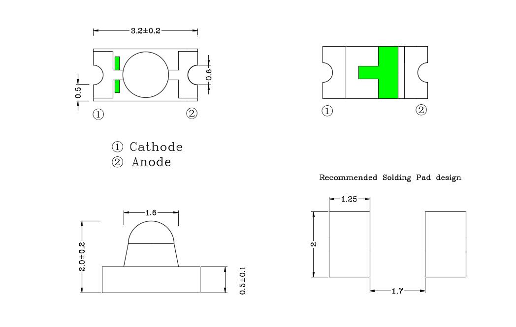
1206 SMD Package Dimensions
The 1206ULM850-L uses a compact surface-mount package. According to the original external dimension drawing, terminal 1 is the cathode and terminal 2 is the anode. The datasheet also provides a recommended soldering pad design for PCB integration.
| Package Parameter | Dimension |
|---|---|
| Package Length | 3.2 ± 0.2 mm |
| Overall Height | 2.0 ± 0.2 mm |
| Base Height | 0.5 ± 0.1 mm |
| Terminal 1 | Cathode |
| Terminal 2 | Anode |
Absolute Maximum Ratings
The following values are the absolute maximum ratings specified in the original datasheet and should not be interpreted as recommended continuous operating conditions.
| Parameter | Rating |
|---|---|
| Continuous Forward Current | 12 mA |
| Maximum Reverse Bias Voltage | 8 V |
| Storage Temperature Range | -40°C to +125°C |
| Substrate Temperature During Operation | -40°C to +90°C |
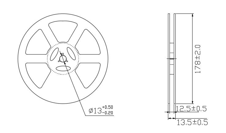
Tape and Reel Packaging
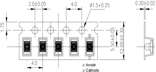
The 1206ULM850-L is supplied in tape-and-reel packaging with 1500 pieces per reel. The original reel and carrier tape dimensions are shown below for production and automated surface-mount assembly reference.
Storage and Handling
The product datasheet specifies moisture-controlled storage requirements before and after opening the package. Following the stated storage conditions helps protect the device before PCB mounting and soldering.
- Do not open the moisture-proof bag before the devices are ready for use.
- Before opening, store at 30°C or below and 60% RH or below.
- The maximum storage period before opening the package is 1 year.
- After opening, keep the devices at 30°C / 35% RH or below.
- Use the devices within 7 days after opening.
- If baking is required before mounting, the specified condition is 60 ± 5°C for 12 hours.
Soldering Precautions
Proper soldering and electrical handling are important for maintaining device reliability. The datasheet specifies the following precautions for mounting and circuit integration.
- Reflow soldering should not be performed more than two times.
- Do not apply mechanical stress to the device during soldering.
- Do not warp the circuit board before it has returned to normal ambient conditions after soldering.
- Use an appropriate current-limiting resistor to keep the device within the rated current.
- Avoid instantaneous high voltage during circuit turn-on and turn-off.
Request a Quote
Contact LumiLaserChip for pricing, sample availability, lead time and technical information for the 1206ULM850-L 850nm 1206 SMD VCSEL. When requesting a quotation, please provide your required quantity, application and relevant technical requirements so that we can evaluate the appropriate supply option for your project.
