

SMD and TO-can VCSELs use the same fundamental VCSEL laser architecture but solve different OEM integration problems. An SMD VCSEL is optimized for PCB-level assembly, compact size, automated pick-and-place and high-volume manufacturing. A TO-can VCSEL provides a discrete mechanical package with pins, an optical window and, in suitable designs, additional space for thermal-control components such as a TEC or thermistor.
The most important distinction is:
- VCSEL describes the laser architecture.
- SMD and TO-can describe package and mounting strategy.
So the question is not whether SMD or TO-can produces a “better VCSEL.” The better package is the one that matches the OEM product architecture.
A practical first rule is:
Choose an SMD VCSEL when PCB-level assembly, compact size, automated manufacturing and high production volume are priorities. Choose a TO-can VCSEL when mechanical protection, easier optical prototyping, defined package geometry or additional thermal-control capability are more important.
This guide compares SMD and TO-can VCSEL packages from the perspective of sensing, datacom, precision optics and OEM manufacturing.
For the underlying VCSEL structure, DBR mirrors and working principle, first see What Is a VCSEL? How Vertical-Cavity Surface-Emitting Lasers Work.
SMD VCSEL vs TO-Can VCSEL at a Glance
| Factor | SMD VCSEL | TO-Can VCSEL |
|---|---|---|
| Laser architecture | VCSEL | VCSEL |
| Mounting method | PCB surface mount | Mechanical / through-pin integration |
| Assembly method | Pick-and-place + reflow | Component insertion / mechanical mounting |
| Footprint | Very compact | Usually larger |
| High-volume production | Strong fit | Good for lower-volume or specialized builds |
| Tape-and-reel | Common | Less typical |
| PCB integration | Excellent | Requires separate mechanical/electrical integration |
| Mechanical protection | Package-dependent | Typically strong |
| Hermetic options | Package-dependent | Common option depending on design |
| Integrated TEC | Usually limited by size | Easier in suitable TO packages |
| Optical window | Package-specific | Common |
| Thermal path | Through package and PCB | Through submount/header to mount or heatsink |
| Prototyping | Requires PCB or carrier | Easy to mount and test mechanically |
| Precision wavelength control | Possible with system design | Strong when TEC-stabilized configuration is used |
| Typical fit | Datacom, proximity, 3D sensing, high-volume modules | Precision sensing, spectroscopy, laboratory and thermally controlled systems |
This comparison is about packaging and integration, not a direct comparison of wavelength, power or spectral performance.
A 940 nm SMD VCSEL and a 795 nm TO-can VCSEL are designed for different optical jobs, so their optical specifications should not be compared as if the package alone created the performance difference.
What Is an SMD VCSEL?
An SMD VCSEL combines a vertical-cavity surface-emitting laser chip with a surface-mount package designed for PCB assembly.
The typical integration path is:
VCSEL Chip → SMD Package → Tape & Reel → Pick-and-Place → Reflow → PCB
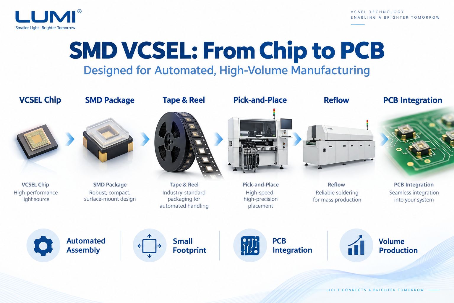
The package normally provides:
- Mechanical support for the VCSEL die
- Electrical pads for surface mounting
- Defined optical aperture
- Compact package geometry
- Compatibility with automated PCB assembly
This packaging strategy is particularly valuable when the laser is part of a larger electronic sensing module rather than a stand-alone optical component.
Why SMD VCSELs Fit PCB-Level Manufacturing
Pick-and-Place Assembly
Surface-mount packages can be placed automatically by standard SMT equipment.
This reduces manual handling and supports repeatable high-volume production.
Tape-and-Reel Supply
SMD components can be supplied in carrier tape and reels, allowing them to feed directly into production equipment.
Lumi’s 850nm 1206 SMD VCSEL – 1206ULM850-L is supplied in tape-and-reel packaging with 1500 pieces per reel and is designed for automated surface-mount assembly. The device is specified as Moisture Sensitivity Level L3 and includes recommended soldering-pad information for PCB integration.
Reflow Soldering
The laser package can be mounted during the PCB reflow process when the part is designed and qualified for the intended solder profile.
For an optical component, however, reflow is not only an electrical process.
The OEM should also consider:
- Maximum package temperature
- Time above liquidus
- Moisture handling
- Optical-window contamination
- PCB warpage
- Solder-joint consistency
Small Footprint
SMD packaging keeps the source close to the PCB and minimizes the mechanical volume around the emitter.
That is particularly useful for:
- Mobile sensors
- Wearables
- Compact proximity modules
- 3D sensing
- Datacom transmitters
- Embedded industrial sensors
Close Driver Placement
The VCSEL driver can be placed close to the emitter.
This can help reduce parasitic effects in applications that use:
- Fast modulation
- Short pulses
- High-speed communication
- Time-of-flight transmission
However, the package alone does not determine bandwidth. The VCSEL chip, package parasitics, PCB layout, driver and operating bias all contribute to the final electrical and optical response.
Lumi 850 nm SMD VCSEL Example
The 1206ULM850-L illustrates why SMD packaging is attractive for high-speed PCB-level integration.
Key characteristics include:
| Parameter | Specification |
|---|---|
| Package | 1206 SMD |
| Typical wavelength | 850 nm |
| Wavelength range | 830–860 nm |
| Typical optical output | 2 mW at 6 mA |
| 3 dB modulation bandwidth | Minimum 3 GHz at 6 mA |
| Typical viewing angle | 12° |
| Moisture sensitivity | MSL L3 |
This is a package-and-application example, not a universal specification for all SMD VCSELs.
The important packaging lesson is that the VCSEL can be handled as a PCB component rather than as a mechanically mounted optical can.
What Is a TO-Can VCSEL?
A TO-can VCSEL mounts the VCSEL die inside a transistor-outline metal package with a header, pins and an optical cap or window.
A simplified construction is:
VCSEL Chip → Submount → Wire Bond → TO Header → Cap / Optical Window → Pins
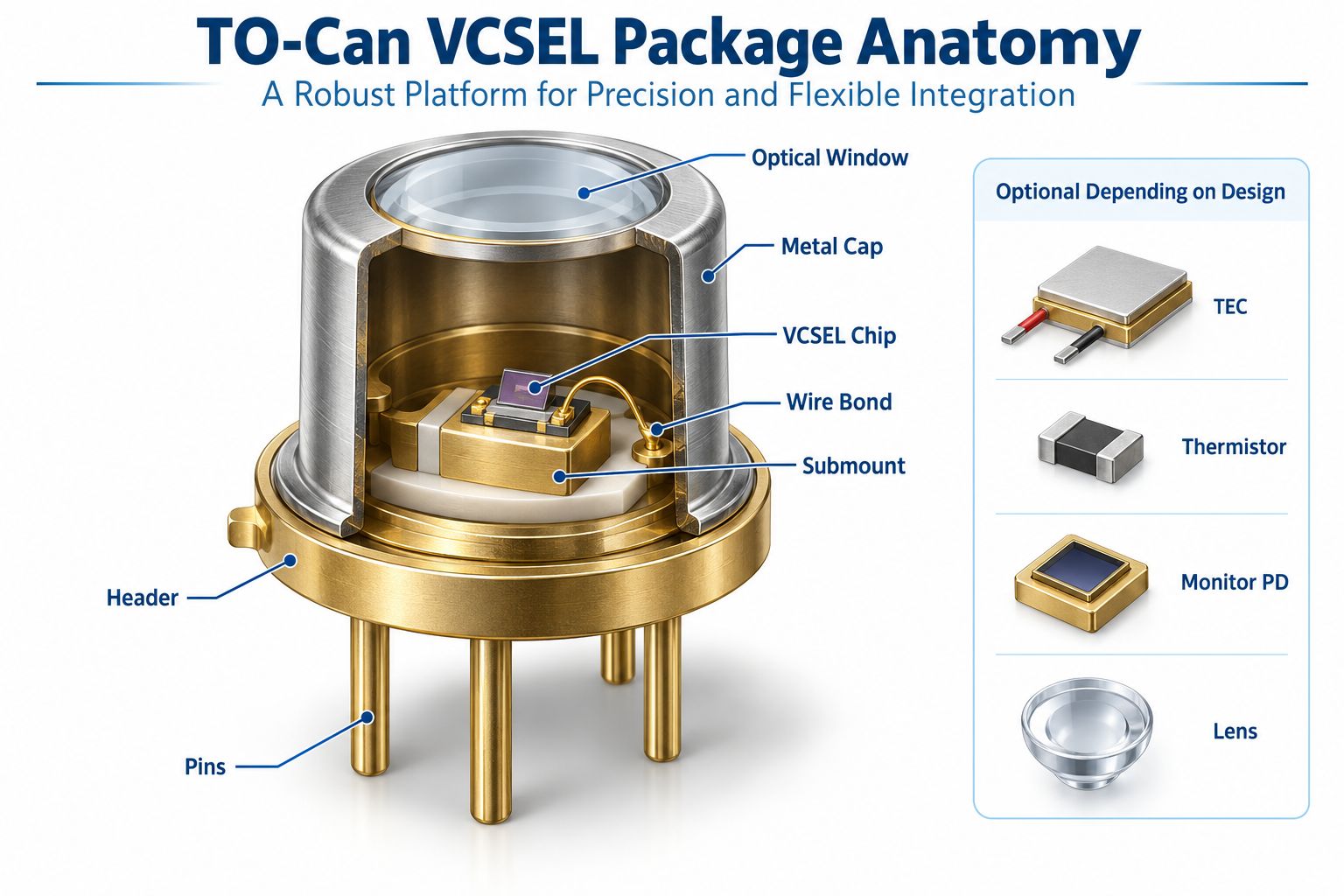
Depending on the design, a TO-can VCSEL can include:
- Metal cap
- Optical window
- Submount
- Wire bonds
- Multiple electrical pins
- Thermistor
- Monitor photodiode
- TEC
- Lens or other optical element
Not every TO-can contains all of these features.
The value of the package is that it gives the VCSEL a well-defined discrete optical and mechanical interface.
Why TO-Can VCSELs Still Matter
TO packaging is sometimes viewed as older than SMD, but that is the wrong way to compare them.
TO-can and SMD solve different manufacturing problems.
Mechanical Robustness
A metal header and cap provide a strong physical structure around the semiconductor die.
This can be useful for:
- Laboratory equipment
- Precision optical modules
- Industrial systems
- Prototypes
- Mechanically adjustable optical assemblies
Optical Window
The package can provide a defined output window.
The OEM can then align:
- Collimator
- Lens
- Fiber coupler
- Spectroscopy optics
- Optical pump path
relative to a repeatable mechanical reference.
Hermetic Packaging Options
TO technology is well suited to sealed package designs when contamination or moisture control matters.
However:
TO-can does not automatically mean hermetic.
Hermeticity depends on the actual product design and sealing process.
Easier Optical Prototyping
A TO device can often be mounted in a socket, mechanical holder or temperature-controlled fixture without first designing a final production PCB.
This makes it attractive during optical R&D.
More Room for Thermal-Control Functions
Larger TO formats can provide more room for:
- TEC
- Thermistor
- Larger submount
- Thermal spreader
This is useful when the VCSEL wavelength is temperature-sensitive and the application requires tighter control.
Lumi 795 nm TO-Can VCSEL Example
Lumi’s 795nm VCSEL Laser Diode with TEC – TO-46 / TO-39 demonstrates this packaging direction.
The device can be supplied in:
- TO-46
- TO-39
- TEC-stabilized configurations
Its typical optical and spectral specifications include:
| Parameter | Specification |
|---|---|
| Typical wavelength | 795 nm |
| Typical output power | 0.13 mW |
| Typical threshold current | 0.75 mA |
| Maximum spectral linewidth | 100 MHz |
| Minimum FM modulation bandwidth | 3.4 GHz |
| Minimum SMSR | 20 dB |
| Minimum PER | 15 dB |
The package options are intended to support different mechanical and thermal integration requirements.
This product should not be compared directly with an 850 nm or 940 nm SMD VCSEL solely on output power or bandwidth. It operates at a different wavelength and is aimed at a different precision-optics use case.
The relevant comparison here is the packaging strategy:
TO-46 / TO-39 + optional TEC versus compact PCB-mounted SMD.
SMD vs TO-Can Thermal Path
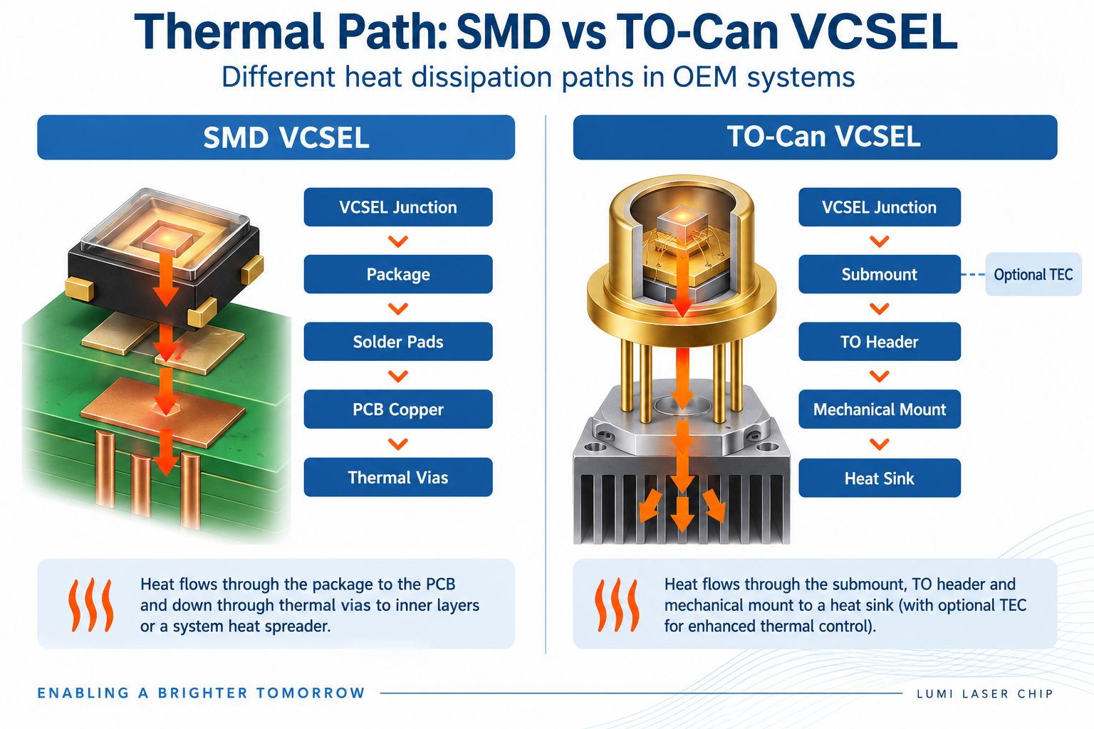
Thermal design is one of the biggest package-level differences.
SMD VCSEL Thermal Path
A simplified SMD thermal path is:
VCSEL Junction → Package → Solder Pads → PCB Copper → Thermal Vias → System
The PCB therefore becomes part of the laser thermal system.
Important design factors include:
- Copper area
- Pad geometry
- Copper thickness
- Thermal vias
- PCB layer stack
- Nearby heat-generating devices
- Ambient temperature
- VCSEL duty cycle
- Pulse current
- Board airflow or enclosure design
A physically small package can still create significant thermal-management requirements if the VCSEL is driven hard or operated continuously.
TO-Can VCSEL Thermal Path
A simplified TO thermal path is:
VCSEL Junction → Die Attach / Submount → TO Header → Mechanical Mount → Heat Sink → System
This architecture allows the OEM to connect the package directly to a defined thermal mount.
When a TEC is integrated, the thermal chain becomes more complex:
VCSEL → TEC → Package Base → External Heat Sink
A TEC improves temperature control, but it does not eliminate the need for system cooling.
The heat pumped by the TEC plus its electrical dissipation still needs to leave the package.
Which Thermal Strategy Is Better?
Neither is universally better.
SMD Is Attractive When
- Power is moderate
- PCB copper can remove the heat
- Duty cycle is controlled
- Module size matters
- SMT manufacturing is a priority
TO-Can Is Attractive When
- A dedicated mechanical heat sink is easier to implement
- Temperature stabilization is important
- TEC integration is required
- Optical alignment hardware already uses a mechanical mount
The thermal solution should therefore be designed at module level, not selected based only on the package outline.
PCB Assembly vs Mechanical Optical Assembly
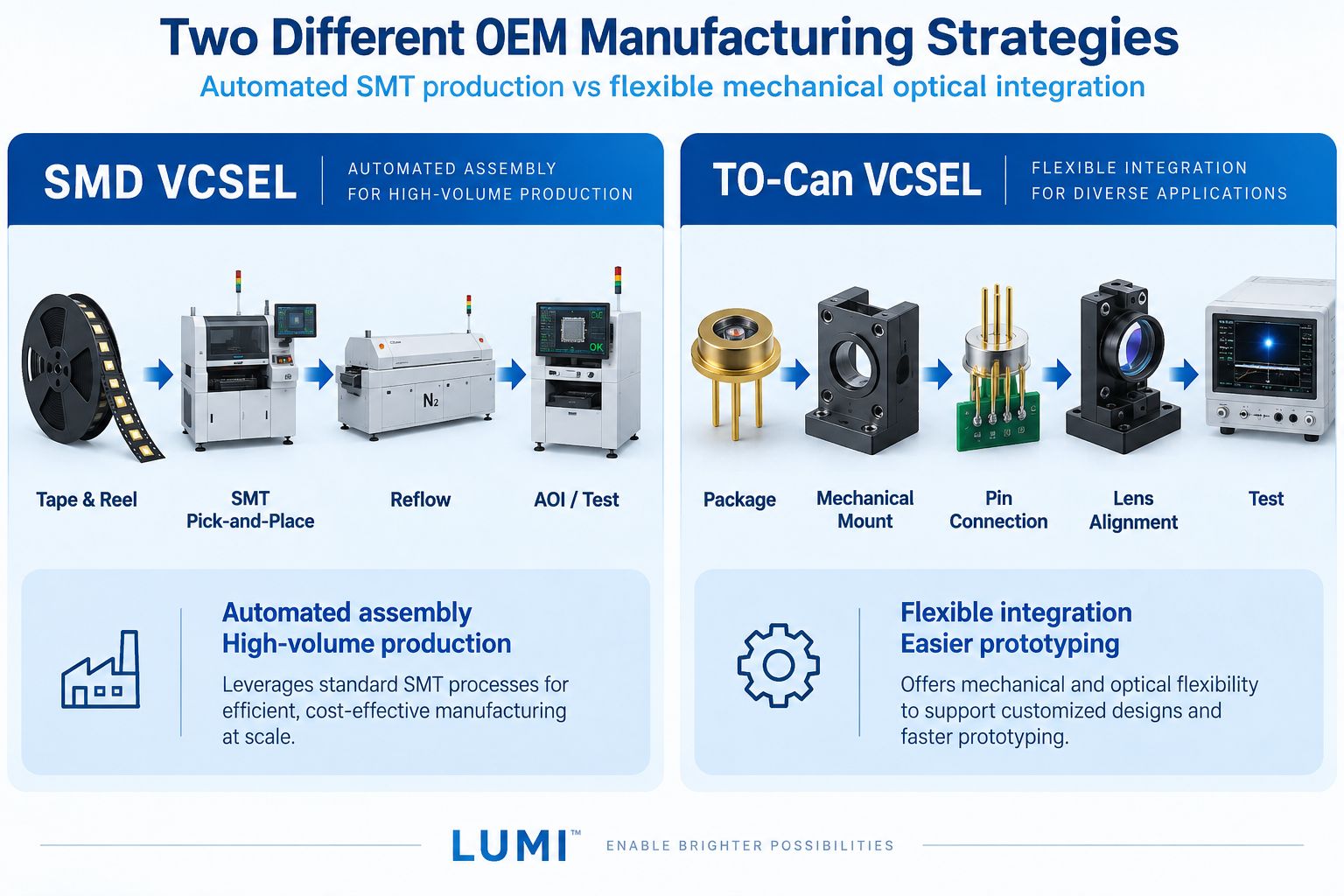
SMD and TO-can packages naturally lead to different OEM manufacturing strategies.
SMD Manufacturing Flow
A typical high-volume process can be:
Tape & Reel → Pick-and-Place → Reflow → AOI / Electrical Test → Optical Module Test
This model fits standard electronics manufacturing.
Advantages include:
- High throughput
- Reduced manual handling
- Repeatable placement
- Lower labor per unit at scale
- Easier integration with other PCB components
This becomes especially valuable at volumes where manual assembly is no longer practical.
TO-Can Integration Flow
A typical TO-based process may be:
TO Package → Mechanical Mount → Pin Connection → Lens / Optical Alignment → Test
Depending on the application, the OEM may also add:
- Temperature-controlled mount
- Collimator
- Fiber coupler
- Detector
- Optical isolator
- Beam steering optics
This process can involve more mechanical assembly, but it provides flexibility during optical development.
Prototyping vs Mass Production
This leads to a practical development observation:
A project may begin with a TO-can VCSEL during optical prototyping and later move toward an SMD VCSEL when the PCB, optics and production architecture become fixed.
That is not always the correct path, but it is a common engineering logic.
TO packaging can be convenient when engineers need to change:
- Lens position
- Heat sink
- Driver
- Optical path
- Temperature control
SMD becomes more attractive when the module architecture is mature and production efficiency becomes a major objective.
Package Size vs Total System Size
SMD is normally the smaller package.
But the smaller package does not automatically produce the smallest finished module.
An SMD design may still require:
- PCB thermal copper
- Lens holder
- Diffuser
- DOE
- Optical shield
- Driver
- Detector
- Mechanical enclosure
A TO package is physically larger but may provide:
- Defined window
- Mechanical datum
- TEC
- Thermistor
- Established mount
- Easier collimator alignment
So:
Compare the complete sensing-module footprint, not package dimensions alone.
This is especially important when the external optics occupy more volume than the VCSEL itself.
Environmental Protection
Package choice also affects how the optical emitter is protected.
SMD VCSEL
An SMD device is often used inside an enclosed electronic module.
The complete product may depend on:
- PCB enclosure
- Lens cover
- Optical shield
- Controlled manufacturing environment
The optical aperture itself still needs to remain clean.
Moisture handling can also matter before reflow. For example, Lumi’s 850 nm 1206 device is specified as MSL L3, so manufacturing storage and soldering procedures should follow the part’s actual handling requirements.
TO-Can VCSEL
A TO package can provide a more enclosed metal-and-window structure around the VCSEL die.
This can be useful when:
- Optical contamination is a concern
- Mechanical handling is frequent
- Laboratory mounting is required
- The package is exposed before final enclosure
- Sealed construction is required
Again, the actual environmental rating should be confirmed from the specific product specification.
Optical Alignment and Lens Integration
VCSELs emit perpendicular to the wafer surface, but the package still determines how the rest of the optical system is built around that beam.
SMD VCSEL Optical Stack
A common SMD sensing module may look like:
VCSEL → SMD Optical Aperture → Lens / Diffuser / DOE → Target
This is well suited to:
- Proximity sensing
- Structured light
- Time-of-flight
- Flood illumination
- Compact datacom optics
The optical stack can be assembled directly above the PCB.
This supports very small module heights but requires tight control of:
- PCB placement
- Optical-axis alignment
- Lens height
- Mechanical tolerance
- Package tilt
TO-Can VCSEL Optical Stack
A TO-based system may look like:
VCSEL → Optical Window → External Lens / Collimator → Optical System
This makes it easier to use:
- Adjustable lens mounts
- Optical benches
- Precision collimators
- External fiber couplers
- Research optics
The TO package therefore remains attractive when the optical geometry is still being tuned or requires mechanical adjustment.
High-Speed Electrical Design
SMD packaging can be especially attractive when high-speed drive signals must travel only a short distance between the driver and VCSEL.
Potential advantages include:
- Short PCB traces
- Close driver placement
- Lower interconnect inductance
- Controlled impedance
- Compact ground return
This can benefit:
- Datacom
- Fast ToF pulses
- High-speed modulation
- Compact optical transmitters
Lumi’s 850 nm 1206 SMD VCSEL provides a minimum 3 GHz 3 dB modulation bandwidth at 6 mA, showing how a compact SMD VCSEL can support high-speed optical integration.
But:
SMD packaging alone does not guarantee higher bandwidth.
Bandwidth still depends on the VCSEL chip, package parasitics, driver, PCB layout, bias point and temperature.
Which Package Fits 850 nm Datacom?
For a compact board-level 850 nm transmitter, SMD is often a strong starting point.
Reasons include:
- PCB mounting
- Short electrical path
- Compact package
- Automated assembly
- High-volume production
- Compatibility with compact multimode-fiber transmitter modules
Lumi’s 850nm 1206 SMD VCSEL is specifically designed for compact surface-mount optical integration.
TO-can VCSELs can also be used in optical communication, but an SMD package is often more convenient when the transmitter is integrated directly into a compact PCB module.
Which Package Fits 940 nm Proximity and 3D Sensing?
For compact 940 nm sensing modules, SMD is also a strong starting point.
Typical reasons include:
- Small footprint
- PCB assembly
- High-volume production
- Compact lens stack
- Integration with detectors and control electronics
Lumi’s 940nm 1616 SMD VCSEL & Photodiode – 1616VCA940R8-PD0224-Z integrates a 940 nm VCSEL and a photosensitive diode inside the same 1616 SMD package.
This is a useful example of how SMD packaging can combine emitter and detector functionality in a very small PCB-mounted device.
The VCSEL section provides a typical optical output of 7.2 mW at 10 mA, while the integrated detector adds optical-sensing functionality within the same package.
Which Package Fits Precision VCSEL Sensing?
For precision wavelength-controlled applications, TO-can can become more attractive when the package needs to support thermal stabilization or adjustable external optics.
Lumi’s 795 nm VCSEL demonstrates this type of use case with:
- TO-46 option
- TO-39 option
- TEC-stabilized configurations
- 100 MHz maximum spectral linewidth
- 3.4 GHz minimum FM modulation bandwidth
- 0.055 nm/K typical wavelength temperature coefficient
Typical application directions include:
- Precision spectroscopy
- Optical pumping
- Frequency-modulated optical systems
- Research instrumentation
- OEM photonics modules
This does not mean TO packaging inherently creates narrow linewidth.
The optical performance comes from the VCSEL design, while the TO + TEC package helps the system control temperature and integrate the source mechanically.
VCSEL Package Fit for OEM Applications
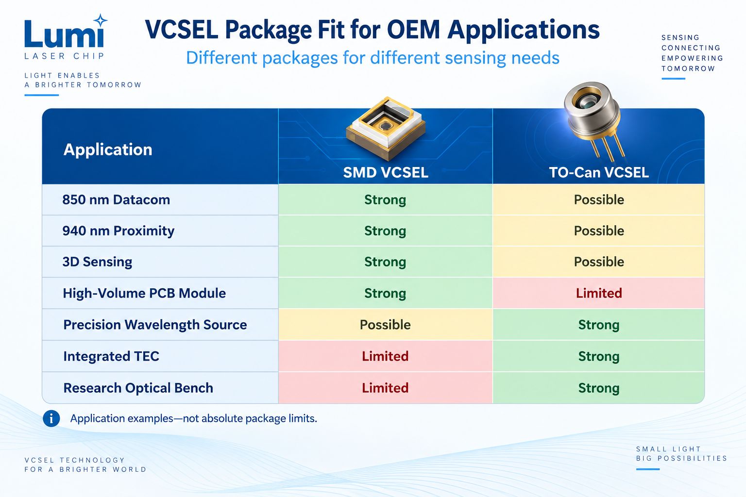
| OEM Application | SMD VCSEL | TO-Can VCSEL |
|---|---|---|
| 850 nm datacom | Strong fit | Possible |
| 940 nm proximity sensing | Strong fit | Possible |
| 3D sensing | Strong fit | Possible |
| High-volume PCB module | Strong fit | Limited |
| Precision wavelength source | Possible | Strong fit |
| Integrated TEC | Limited by compact package | Strong fit in suitable TO design |
| Research optical bench | Possible | Strong fit |
| Adjustable external optics | Possible | Strong fit |
| Compact emitter + photodiode | Strong fit | Application-dependent |
| Mechanically rugged discrete source | Possible | Strong fit |
These are application examples, not absolute package limits.
A custom SMD design can support requirements beyond this table, and a TO package can also be used in high-volume applications when the system architecture justifies it.
Cost: Compare Assembly Cost, Not Only Laser Price
Package cost is only one part of the system economics.
SMD Cost Structure
SMD can reduce:
- Manual placement
- Hand soldering
- Mechanical fixtures
- Per-unit assembly labor
But it may require investment in:
- SMT process development
- Stencil design
- Reflow profiling
- Moisture handling
- PCB qualification
- Automated optical inspection
- Production test fixtures
At high volume, these investments can be spread across many units.
TO-Can Cost Structure
A TO package can involve:
- Higher discrete package cost
- Mechanical mount
- Manual or semi-automated insertion
- Lens alignment
- Socket or fixture
- External heat sink
However, for engineering prototypes, low-volume instruments, research systems and custom precision optics, the TO approach can reduce development complexity because the laser is easier to mount and reconfigure.
The lower-cost package is not necessarily the lower-cost system.
Evaluate total assembly, optics, test and thermal-control cost.
Is TO-Can More Reliable Than SMD?
Not automatically.
Reliability depends on:
- Die quality
- Package design
- Moisture protection
- Wire bonds
- Solder joints
- Thermal cycling
- Mechanical stress
- Optical contamination
- Drive current
- Junction temperature
TO packages can offer strong mechanical and environmental protection, while a well-designed SMD package can also provide excellent reliability in high-volume electronics.
The package should be qualified for the actual operating environment.
Does TO-Can Always Mean Hermetic?
No.
TO-can technology is well suited to hermetic sealing, but not every TO product is hermetic.
If hermeticity matters, request:
- Package sealing specification
- Leak-test information
- Environmental qualification
- Applicable reliability data
Do not infer hermetic performance from the metal can alone.
Can the Same VCSEL Architecture Use Different Packages?
Yes.
The same fundamental VCSEL architecture can be integrated into different package families depending on:
- Chip dimensions
- Electrical contacts
- Thermal requirements
- Optical aperture
- Target production process
- Custom package design
This is why VCSEL should always be separated conceptually from its package.
For a broader package framework, see Laser Diode Package Types: TO-Can, Butterfly, SMD & Fiber-Coupled Output Explained.
How to Choose Between SMD and TO-Can VCSEL
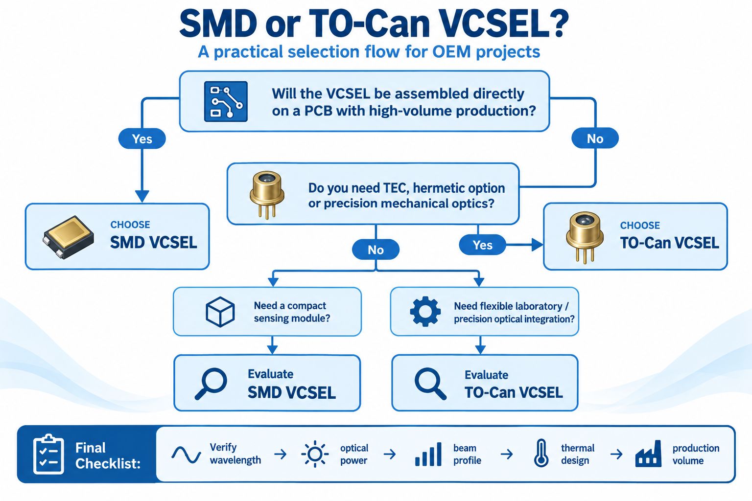
A practical selection sequence is:
1. Will the VCSEL Be Assembled Directly onto a PCB?
If yes, especially in high volume:
Start with SMD.
2. Do You Need Tape-and-Reel and Automated Reflow?
If yes:
SMD is the natural manufacturing format.
3. Do You Need a Defined Mechanical Optical Package?
If yes:
Evaluate TO-can.
4. Is Integrated TEC or Tight Thermal Stabilization Required?
If yes:
TO-can is often the stronger starting point, especially where a larger package can accommodate a TEC and thermistor.
5. Is the System a Compact Proximity, ToF or 3D-Sensing Module?
If yes:
SMD is usually the stronger starting point.
6. Is the System a Laboratory, Spectroscopy or Precision Optical Platform?
If yes:
TO-can may simplify mechanical and thermal integration.
Then verify:
- Wavelength
- Optical power
- Beam divergence
- Spectral behavior
- Modulation bandwidth
- Thermal design
- Optical stack
- Operating temperature
- Production volume
Common SMD vs TO-Can Selection Mistakes
Mistake 1: Assuming VCSEL and SMD Mean the Same Thing
VCSEL is the laser architecture. SMD is a package.
Mistake 2: Assuming TO-Can Is Outdated
TO packaging remains useful for precision optics, laboratory integration, thermal stabilization and mechanically robust optical systems.
Mistake 3: Choosing SMD Only Because It Is Smaller
The external lens, PCB, heat-spreading copper and enclosure may dominate the total module size.
Mistake 4: Choosing TO Only Because It Looks More Rugged
Mechanical robustness is useful only if it solves a real system requirement.
Mistake 5: Ignoring PCB Thermal Resistance
An SMD VCSEL uses the PCB as part of the thermal path.
Mistake 6: Ignoring Reflow and Moisture Handling
SMD optical components require controlled assembly conditions.
Mistake 7: Comparing Lumi’s 850/940 nm SMD Products Directly with the 795 nm TO Product
These products target different wavelengths and applications.
Their differences in optical power, linewidth and modulation are not caused solely by SMD versus TO packaging.
Use them as packaging examples, not as a one-to-one optical-performance benchmark.
Lumi VCSEL Packaging Examples
850 nm 1206 SMD VCSEL
The 1206ULM850-L is a compact high-speed SMD VCSEL designed for PCB-level optical integration.
It is a strong example of:
VCSEL architecture + SMD package + high-volume assembly
940 nm 1616 SMD VCSEL + Photodiode
The 1616VCA940R8-PD0224-Z integrates the emitter and photosensitive diode within one compact SMD component.
It illustrates:
VCSEL + detector integration + PCB-level package
795 nm TO-46 / TO-39 VCSEL with TEC Option
The 795nm VCSEL Laser Diode is available with TO-46, TO-39 and TEC-stabilized package options.
It illustrates:
VCSEL architecture + discrete mechanical package + thermal-control option
For the broader product family, see the VCSEL Laser Diode category.
For neutral background on common laser-diode packaging considerations, Wavelength Electronics provides an application note covering TO-can and other package families: Common Laser Diode Packages.
Frequently Asked Questions
What is the difference between an SMD VCSEL and a TO-can VCSEL?
Both use VCSEL laser architecture. The main difference is packaging and OEM integration. SMD is optimized for PCB surface mounting and automated production, while TO-can provides a discrete metal package with pins, optical-window options and greater flexibility for mechanical or thermal integration.
Is SMD a type of VCSEL?
No. SMD describes the package and mounting format. VCSEL describes the semiconductor laser architecture.
Can the same VCSEL chip be packaged in SMD or TO-can?
Potentially yes, if the die design, electrical contacts, optical geometry and thermal requirements are compatible with both package designs.
Is TO-can more reliable than SMD?
Not automatically. Reliability depends on the die, package materials, sealing, solder joints, thermal cycling, drive conditions and final system environment.
Can a TO-can VCSEL include a TEC?
Yes. Larger TO configurations can support TEC-based temperature stabilization. Lumi’s 795 nm VCSEL is available in TO-46 / TO-39 and TEC-stabilized configurations.
Which VCSEL package is better for 3D sensing?
For compact, high-volume PCB-based 3D-sensing modules, SMD is often the stronger starting point because it supports automated assembly and a compact optical stack. The final choice still depends on power, optics, thermal requirements and volume.
Which package is better for high-volume production?
SMD is generally stronger for standard SMT-based high-volume PCB production because it supports tape-and-reel, pick-and-place and reflow assembly.
Which package is easier for prototyping?
TO-can is often easier for optical-bench and mechanically adjustable prototypes because it can be mounted independently of a final production PCB. SMD evaluation boards can also simplify early development.
Is a TO-can VCSEL hermetic?
It can be, but not every TO-can is hermetic. Hermeticity must be confirmed from the actual product specification.
Should I choose the package before choosing the wavelength?
No. Define wavelength, optical power, beam, spectral behavior and modulation first. Then choose the package that supports the required mechanical, thermal and manufacturing strategy.
Same VCSEL Architecture, Different OEM Strategy
SMD and TO-can are not competing laser technologies.
They are two different ways of turning a VCSEL chip into an OEM-ready component.
Choose SMD when the product is driven by:
- Compact PCB integration
- Tape-and-reel
- Automated pick-and-place
- Reflow assembly
- High production volume
- Short electrical paths
- Compact sensing modules
Choose TO-can when the product benefits from:
- Mechanical package robustness
- Defined optical window
- Easier bench prototyping
- Adjustable external optics
- Dedicated heat sinking
- TEC or thermistor integration
- Precision wavelength control
The final decision should combine:
VCSEL wavelength + optical performance + package + thermal path + optical stack + production strategy
rather than treating package size alone as the answer.
Lumi provides VCSEL components in SMD and TO-can configurations for OEM sensing, communication and precision photonics.
Explore the Lumi VCSEL Laser Diode range or contact Lumi with your target wavelength, package, optical power, thermal-control requirement and expected production volume for project evaluation.
