Laser Chip

Empowering Optical Communications and Sensing

Lumi · Laser Chip OEM Factory

Catering to high-speed communication, 3D sensing, consumer electronics, industrial, and automotive applications, we provide a comprehensive suite of end-to-end services—ranging from design support and MPW wafer services to testing, analysis, and packaging solutions—helping customers shorten product introduction cycles and enhance mass production efficiency

Advanced Process Platform
Process Quality Management
Coverage of Multiple Device Types
Global OEM Services

Photodetector

PD / APD / MPD

10G / 25G / 50G
800nm–2600nm
Meets the requirements of silicon photonics, communications, and sensing applications.

Edge-emitting laser

FP / DFB / EML

FP:10G / 25G / 100G / 200G
DFB:1310nm / 1550nm / 1650nm
EML:100G / 200G

Vertical-Cavity Surface-Emitting Laser

VCSEL

850nm 10G–200G
650nm–850nm / 905nm / 940nm
Consumer Electronics and 3D Sensing Applications

Application

Optical Communication

Data Centers / 5G Base Stations / Long-Distance Transmission

Gas Monitoring

Methane / Oxygen / Hydrogen sulfide/Toxic Gases

Consumer Electronics

3D Sensing / Medical Aesthetics / Facial Recognition

Industrial & Medical

Spectral Analysis / Laser Processing / Medical Equipment

Core Technological Advantages

Advanced Epitaxial Technology

• InP / GaAs Epitaxial Growth Platform
• Multiple Quantum Wells / Nano Structures / Butt-Joint Growth
• High Uniformity and Low Defect Density

Precision Process Manufacturing

• Oxidation / Etching / Thin-Film Processes
• Flip-Chip Long-Wavelength Packaging / Bonding Processes
• High-Precision Packaging and Mass Production Capability

Strict Testing & Reliability

• Wafer-Level and Device-Level Full Process Testing
• Aging Test / Low Noise / High Reliability
• Comprehensive Reliability Verification System

Process Platform Edge-Emitting Lasers
(FP / DFB)
Vertical-Cavity Surface-Emitting Lasers
(VCSEL)
Photodetectors
(PD / APD / MPD)
Substrate Material InP / GaAs InP / GaAs InP / GaAs
Epitaxial Material AlGaInAs / InGaAsP / GaInP / InGaAs / InP / AlGaAs GaAs / AlGaAs / InGaAs / InAlGaAs / GaAsP / AlGaAsP InGaAs / InAlAs / AlGaAs / InGaAsP / InAlGaAs
Wafer Size 75mm / 100mm 75mm / 100mm / 150mm 75mm / 100mm

Three Specialized Process Platforms

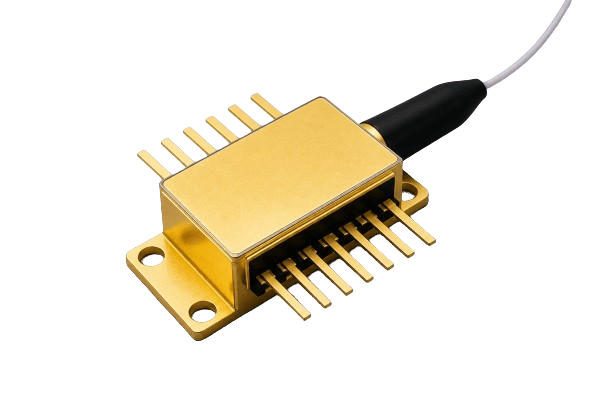
Encompassing edge-emitting lasers, vertical-cavity surface-emitting lasers (VCSELs), and detector platforms, we provide a one-stop foundry solution ranging from design to mass production.

Edge-Emitting Laser Platform

Focused on edge-emitting laser devices for communication and sensing applications, with mature capabilities in epitaxial growth, grating design, and chip fabrication processes.

  • • RWA Structure, BH Structure
    • EBL Gain, CPW Electrodes
    • ECR Thermal-Control Coating
    • Butt-Coupled Integrated Structure

Vertical-Cavity Surface-Emitting Lasers (VCSELs)

Providing full-process VCSEL manufacturing technology, supporting the development of high-power and high-efficiency VCSEL products.

  • • Wet Oxidation Process
    • Vertical Etching Process
    • Polarization VCSEL Grating Process
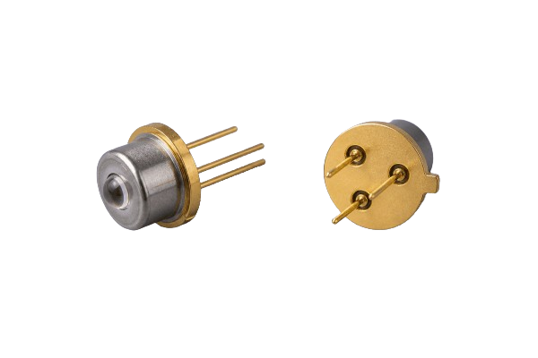
Photodetectors

Covering multiple photodetector process platforms, supporting the development and mass production of high-speed, high-sensitivity photodetector products.

  • • Low-Temperature, High-Uniformity Zinc Diffusion Process Based on MOCVD
    • APD Sidewall Passivation Process and BCB Planarization Process
    • On-Wafer Bandwidth Testing (Up to 67 GHz)

Optoelectronic Epitaxy Process Platform

GaAs Series

905/940 nm Single-Junction / Multi-Junction VCSEL;10G / 25G VCSEL

InP Series

MPD, 10G / 25G / 56G PD;O-band / C-band 10G / 25G FP / DFB;EML, QCL;2.5G / 10G APD, SPAD;High-Power FP / SLD / SOA / DFB

Certification